-
PRODUCTS
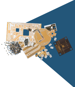
SEMICONDUCTORSdiodes and rectifiersdiscrete thyristorsIC - POWER AND LINEARmosfetsoptoelectronicsPOWER MODULESPASSIVE COMPONENTSinductors and magneticssensorsOther components

-
APPLICATIONS

-
RESOURCES
-
CUSTOM CAPABILITIES
-
Company


Why Vishay Thin Film Solutions?
Excellence in build to print manufacturing services

Cutting-Edge Thin Film Technologies

Advanced Integration Solutions

Engineering Collaboration and Innovation

Rapid Prototyping and Scalable Production

Customer-Focused Engineering Precision

About Thin Film Solutions
Rapid Prototypes Accelerating the path from concept to qualified
0+
Years Experience
Multi-Site Manufacturing to Minimize Supply Risk
High reliability solutions for Aerospace & Defense, Medical and Automotive systems
Our Thin Film Solutions

Case Studies
AESA Radar Interconnect Optimization
Improving mmWave performance by reducing interconnect losses and variation
Challenge
A radar module prototype showed higher than expected insertion loss, unit to unit phase variation, and resonances at operating frequencies beyond 80 GHz. Investigation traced the issue to inductor loss, wire bond inductance, and discrete passives in the RF interconnect path.
Solution
A custom thin film substrate was developed with integrated passive elements and precision-machined pockets, greatly reducing conductor loss, allowing the RF paths to be shortened and parasitic effects to be substantially reduced.
Result
Measured insertion loss improved by approximately 1.0 dB – 1.5 dB, with module to module variation reduced to under ± 0.1 dB. The improved interconnect consistency enabled more stable phased array performance at mmWave frequencies
“Once we tested performance of our original design, it became clear the limitation wasn’t the GaN device—it was everything around it. The thin-film interconnect let us clean up the RF paths and get the repeatability we needed across the array.” — RF Packaging Engineer, Military Radar Program
Miniaturized Implantable Thin Film Module
Supporting high density routing and long term reliability in implantable electronics
Challenge
Next-generation implantable electronics required higher interconnect density, controlled impedance, and long term protection against moisture ingress. Thick film and discrete feedthrough approaches could not meet the required routing density or provide reliable hermetic performance within the available form factor and price point.
Solution
A thin film substrate was implemented on an inert ceramic base using fine-line geometries and tightly controlled tolerances. Hermetic, solid gold-filled vias were used to provide compact vertical interconnects while maintaining a moisture-impermeable signal path.
Result
Line widths below 25 µm enabled higher circuit integration and a reduced module footprint. The integrated hermetic vias provided reliable moisture isolation, improved signal integrity, and repeatable electrical performance.
“Thin film gave us a practical way to increase routing density without compromising long term reliability in an implantable form factor.” — Lead Packaging Engineer, Implantable Medical Device Program
Hermetic Thin Film Feedthroughs for Ka-Band GaN
Enabling low loss RF transitions and improved thermal performance in hermetic packages
Challenge
A high power Ka-band GaN amplifier module for space applications required hermetic packaging to meet environmental and lifetime requirements. Conventional feedthroughs and metal pin transitions introduced excess RF loss and impedance discontinuities at Ka-band frequencies. In parallel, the hermetic enclosure limited heat flow away from the GaN die, driving junction temperatures beyond acceptable margins.
Solution
Working closely with the customer, Vishay supplied a custom thin film substrate fabricated with hermetic, solid gold-filled vias placed directly beneath and around the GaN die. The vias replaced the ring frame with its hermetic feedthroughs, providing a short, low inductance RF transition through the package while also creating direct vertical thermal paths to the backside heat spreader.
Result
RF insertion loss across the hermetic boundary was reduced by approximately 1.0 dB – 1.5 dB, with interconnect inductance reduced by more than 60 %. Improved thermal conduction through the via structure lowered GaN junction temperatures by 15 °C – 25 °C. The approach met space-qualified hermetic requirements while delivering improved RF and thermal performance across flight hardware.
“Hermeticity forced us into compromises we didn’t like—especially at Ka-band. Integrating hermetic RF transitions and thermal paths through the thin film structure let us remove the ring frame and recover performance without giving up package integrity.” — RF Module Lead Engineer, Satellite Payload Program
Passive Optical Alignment & Eutectic Bonding with Thin Film
Enabling scalable, high yield optical module assembly
Challenge
Laser diode modules required precise optical fiber alignment, uniform eutectic bonding, and efficient heat removal. Manual active alignment and paste-based AuSn attachment introduced variability in bond thickness, alignment accuracy, and overall yield, limiting scalability.
Solution
A custom thin film submount, machined passive alignment grooves and fiducials etched directly into the substrate. An AIN base with sputtered AuSn provided heat spreading and a uniform eutectic die attach, while thin film sidewall metallization enabled eutectic bonding of lenses with controlled alignment.
Result
Passive alignment reduced assembly time and improved optical coupling repeatability. The sputtered eutectic process produced void-free bonds with controlled bond-line thickness, improving thermal performance and enabling scalable, high yield optical module production.
“Active alignment worked, but it didn’t scale. By moving the alignment and bonding geometry into the thin film structure, we were able to improve repeatability and get out of the manual tuning loop.” — Optical Module Manufacturing Engineer
Custom Solutions
Vishay's Custom Capability Solutions offer tailored components and assemblies to meet specific customer requirements across diverse industries.
Facing a design challenge?
We offer the technology to help you translate your electrical, thermal, and mechanical requirements into high performance solutions.
About Vishay
While boasting an ever-growing portfolio of discrete semiconductors and passive components, we support the growing needs of our customers by committing to:
Higher capacity readiness
New product releases
Increased technical resources
Vishay is close by:
We operate in every region to meet you wherever you are.

investment in capacity expansion (2024-2028)
Patents
Years of technological leadership in the components industry
Vishay Employees Worldwide

Vishay manufactures one of the world’s largest portfolios of discrete semiconductors and passive electronic components that are essential to innovative designs in the automotive, industrial, computing, consumer, telecommunications, military, aerospace, and medical markets. Serving customers worldwide, Vishay is The DNA of tech.®
CONNECT WITH US


Copyright ©2026 Vishay Intertechnology, Inc.


