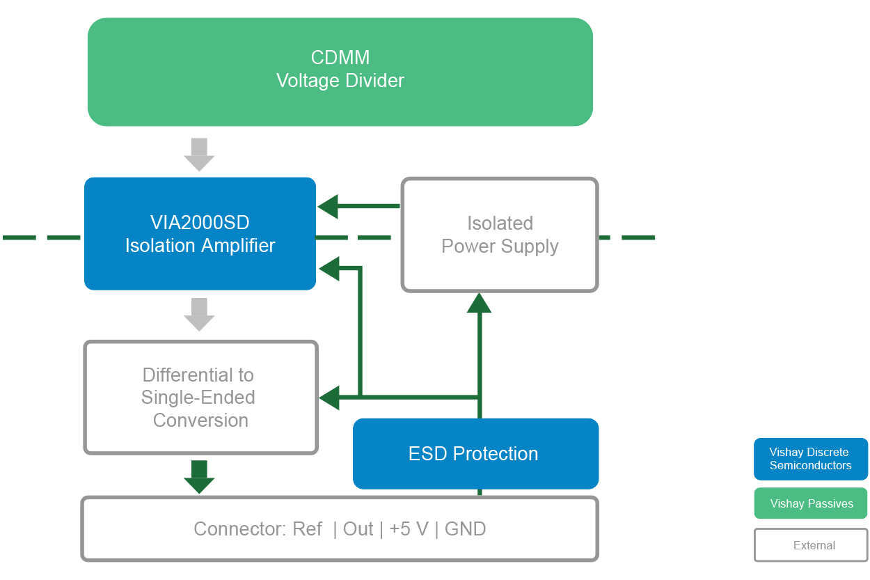
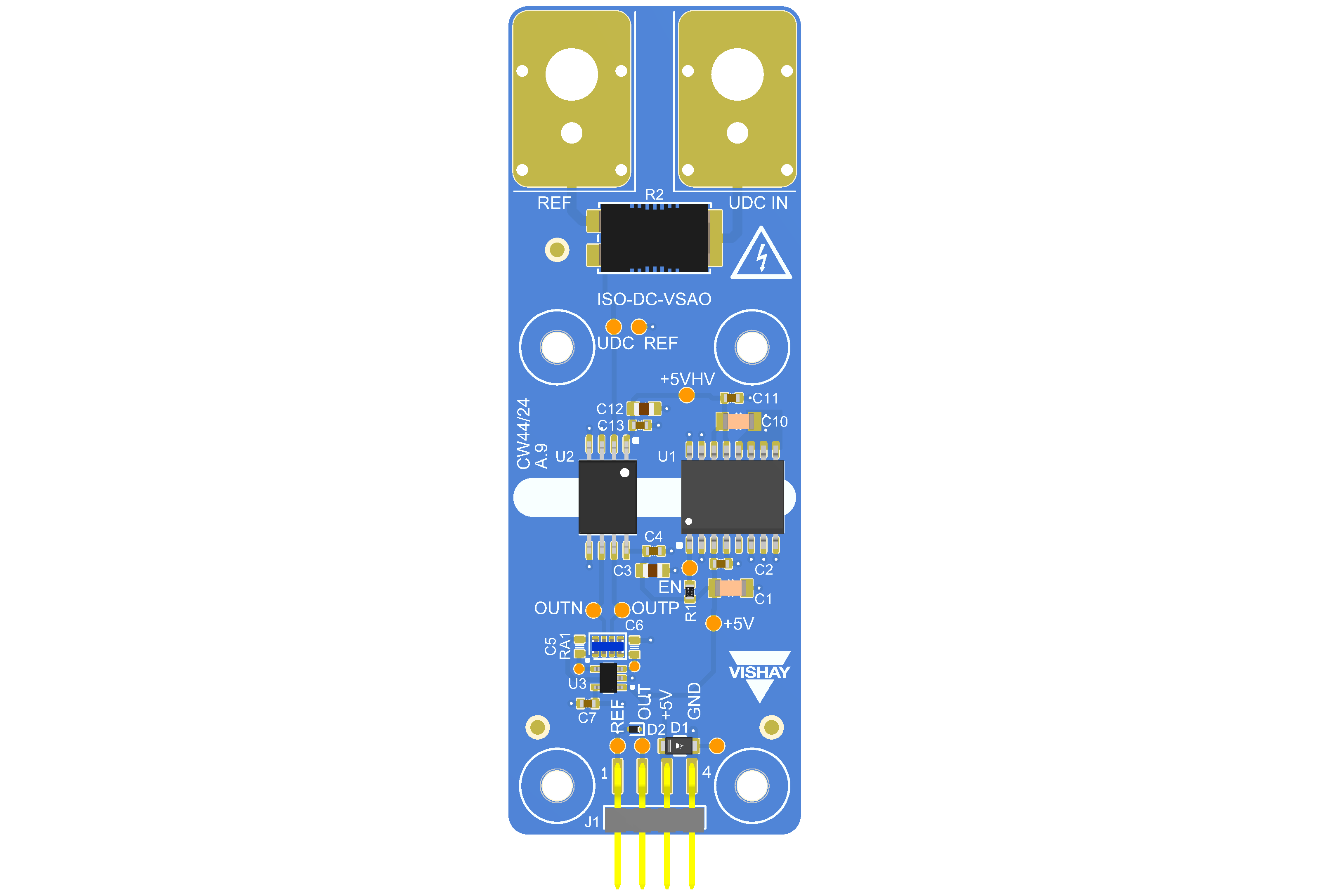
Isolated DC Voltage Sensor with Analog Output

Selected

This application is based on the VIA2000SD isolation amplifier and a CDMM voltage divider. The high voltage input (UDC to REF) is scaled down to +2000 mV (UDC to REF) using a set of CDMM resistors. This reduced voltage is then fed into the VIA2000SD isolation amplifier, which produces an isolated, amplified analog signal at its output (OUT to OUT).

The differential output signal, with a common-mode voltage of 1.44 V, is accessible via pin headers labeled OUT and OUT, allowing users to connect a differential ADC or to use it for other prototyping needs. This differential output is converted to a single-ended output, providing an output in the range from 0 V to 2.5 V (OUT to GND), which is ready to be interfaced by a single-ended ADC or multimeter.

To allow the lowest possible thermal drift, the differential to single-ended conversion stage is based on the ACAS resistor network, providing well-matched resistance values over a wide range of temperatures.

Reference Design Files

Reference Board

Datasheet

Selected

Reference

Functional Block Diagram

Slider

Features

DC voltage measurements up to 1000 VRMS

Maximum working isolation voltage of 1200 VRMS

Isolated single-ended analog output

Low temperature offset and gain drift

Large bandwidth of 290 kHz

Products

Download

All reference designs provided by Vishay Intertechnology, Inc. and its affiliates (collectively “Vishay”) are provided "as is". Vishay makes no warranties or representations with regard to the reference designs or use of the reference designs, express, implied or statutory, including accuracy or completeness. Vishay disclaims any warranty of title and any implied warranties of merchantability, fitness for a particular purpose, quiet enjoyment, quiet possession, and non-infringement of any third-party intellectual property rights with regard to Vishay’s reference designs or use thereof. Vishay shall not be liable for and shall not defend or indemnify buyers against any third-party infringement claim that relates to or is based on a combination of components provided in a Vishay reference design. In no event shall Vishay be liable for any actual, special, incidental, consequential or indirect damages, however caused, on any theory of liability and whether or not Vishay has been advised of the possibility of such damages, arising in any way out of Vishay reference designs or buyer’s use of Vishay reference designs.