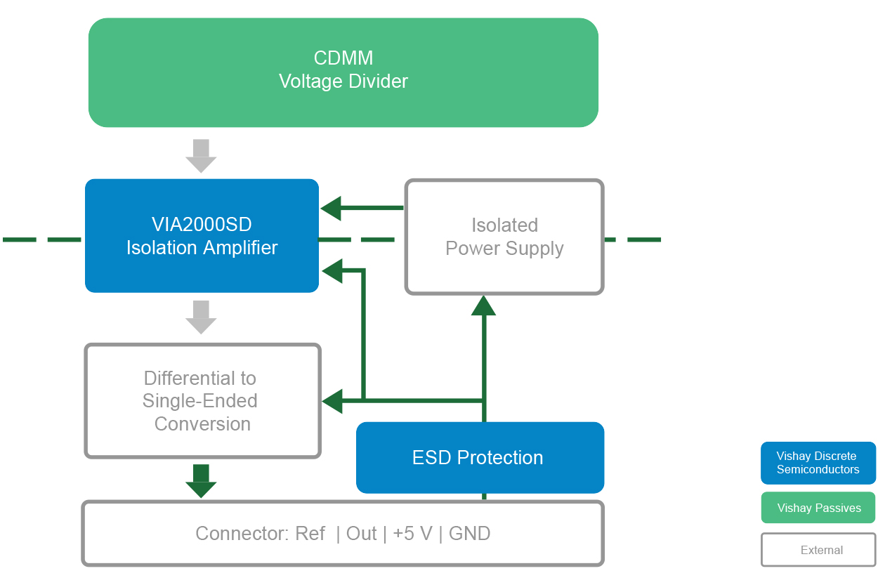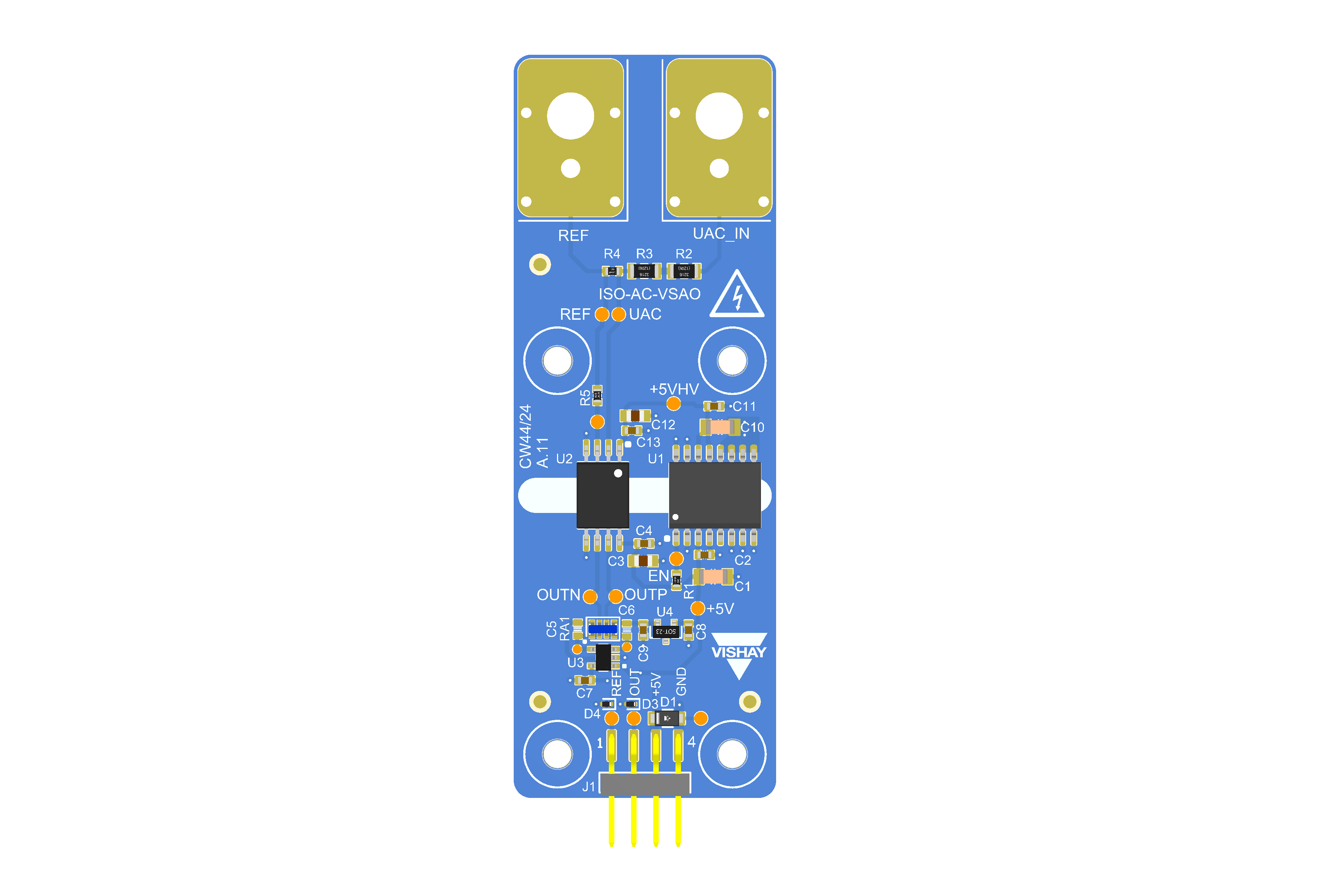
In this design, the signal from a discrete TNPV voltage divideror is fed to a VIA0250DD, a high-performance, isolated, differential output amplifier. The VIA0250DD has a linear differential input range of ±250 mV and a linear differential output range of ±2.05 V, which is converted to a single-ended output ranging from 0 V to 2.5 V (OUT to GND). This output is ready to be interfaced with a single-ended ADC or multimeter.
Using the combination of a discrete voltage divider and a VIA0250DD isolation amplifier, this design provides an analog output for AC current measurement up to ±400 V rms at a bandwidth of ~ 300 kHz.