Vishay's Resistors and Inductors FAQ (RIFAQ) is a collection of detailed answers to questions frequently asked by engineers about the use of these technologies in their designs. For more information or questions, please contact your local Vishay marketing expert.
- What is difference between a copper-clad terminal construction (WSK0612) and a welded copper terminal construction (WSKW0612)?
- A few questions regarding the WFM series datasheet.
- Does the WSL have UL certification?
- Regarding the power derating curve, what's the difference between terminal temperature and ambient temperature?
- The maximum case temperature will reach 141 °C when 2.5 W maximum power is applied to the WSLF2512L5000FEA during the thermal test. Could you please help to determine whether this will result in any thermal risks?
- How is the R value of shunt resistors measured?
- What is a MELF resistor? What are the advantages of using a MELF resistor over a flat chip SMD resistor?
- Can the worst-case resistance value change be calculated or estimated based on the estimated number of hours in operation?
- Apart from long time resistance drift, are there other parameters / conditions to be considered for the worst-case change in the resistance value?
- Why is the Vishay CRCW-HP more robust to pulse surges than competitors' double power mode thick film chip resistors?
- When mounting a MELF resistor on the PCB, what kind of nozzle should be used in the pick and place machine?
- How does a thin film chip resistor prevent a large aging drift of the resistance value in the final product (problem of electrolytic corrosion)?
- There are two MELF operation modes: standard mode and power mode. What is the difference between them and how can I order the correct part?
- If we use the TNPV or MMA HV, how do we ensure that the creepage distance will be all right compared to using a few resistor pieces?
- What is the maximum rated power when a surface-mount thick film power resistor such as the D2TO35 / DTO25 is mounted on an ordinary PCB?
- What is the partial discharge of a power thick film resistor, and what are its effects?
- What are the root causes of partial discharge failure?
- What are the suggestions for customers when performing a partial discharge test?
- The customer wants to know if the LTO150 can withstand 150 W for 0.3s. According to the power curve in the datasheet, it seems that the LTO150 can withstand 450 W in 0.2 s.
- Why do Vishay's metal composite power inductors have lower EMI noise than the competition?
- Are there any precautions to take when mounting metal composite power inductors on the PCB?
- Is conformal coating on inductors permitted? Will it affect quality or reliability?
- What should the storage conditions for the IHLP series be?
- For the IHLP series, is it permissible to exceed the maximum voltage?
- If there are differences in inductor lead lengths, would there be differences in the magnetic / electric field?
- How should I define the differences between IHLP suffixes, like 01(A1), 11(1A), 51(5A), etc.?
- What is the difference between the rated current and saturation current of an inductor?
- Do IHLP inductors have problems with long term stability when working at high temperatures?
- If we cannot find the suitable saturation current in the required size, what should we find next?
- How can we get the Vishay NTC thermistor R-T table?
- At what temperature does the NTCS detect an extreme ambient temperature difference between the top and bottom side?
- Questions about R-T tables.
- Are NTC products sensitive to electrical overstress (EOS) such as ESD, and what capabilities can we suggest?
- How should a NTC resistance value be selected for an application?
- How fast do NTCs respond?
- There are two temperature ranges specified: one at zero power and another at maximum power. What are these for?
- For the NTCS0805 thermistor, the power rating given in the datasheet is 210 mW, while the power rating given for the leaded type is 100 mW. Why is there such a difference?
- How are NTC thermistors measured?
- For the NTCC wire bonding type, will silver plating impact weldability?
- What is the TCR for various resistor element materials?
- What is the recommended soldering profile for axial leaded resistors, such as the CW02 series?
- What information should be considered when reviewing pulse handing resistors?
- What is the meaning of 0.05 Ω in the test limit of ± (5.0 % + 0.05 Ω) ΔR?
- What is the power derating curve of a resistor and what does it mean?
- What is the voltage coefficient of a high voltage resistor?
- What is the difference between discharge and active discharge in EV inverters?
|
Q1. |
What is difference between a copper-clad terminal construction (WSK0612) and a welded copper terminal construction (WSKW0612)? |
|
A1. |
Welded Copper VS. Copper-Clad Terminal
Construction 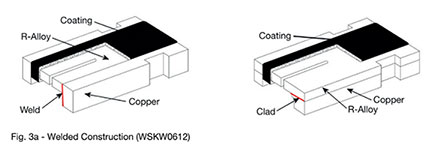
Effects of Clad Construction This has two major effects on performance. First, mounting accuracy is reduced, causing less consistency in resistance values when parts are mounted to a circuit board. This means that it is essential for designers using a thin copper terminal construction to take into account the direction and positioning for the current traces to be presented to the part. The second effect is higher TCR, which may seem counterintuitive because the thin cross-section terminal has less copper in the circuit; however, the higher TCR is caused by how the current distributes into the resistor element. Benefits of Welded Construction This significantly reduces the sensitivity to variations in the board mounting process and insures the most consistent in-circuit measurement performance for all resistance values. Additionally, the welded construction improves the TCR performance by directing current flow more consistently to the resistance element. In short, this construction provides a part that is less sensitive to circuit board design and is more stable across a wide range of operating temperatures, which ultimately results in a more accurate resistor. |
|
Q2. |
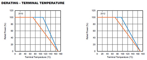
A few questions regarding the WFM series datasheet.
|
|
A2. |
The curves are based on the terminal derated power
listed on page one of the Standard Electrical
specification. Previously it listed 2512 and 2010 on
the same graph with only the highest power rating
listed.
One of the resistive elements used is Ni-Cr, which has superior stability at higher operating temperatures (220 °C) compared to copper manganese alloys (185 °C). This provides two application benefits. First, WFM devices are able to withstand higher temperatures with less lifetime drift. Second, the resistors have improved pulse capability due to a greater element mass for the same resistance value compared to the competitors' alloy. Foil on copper has a higher rated power capability for the same resistance value and provides long term stability. The WFM has a higher resistance range than the WSL and so board shift is not going to be as much of a factor. The low resistance value of the solder connection will contribute a smaller influence on the higher resistance value resistor. Board shift becomes a more significant contributor at 5 mΩ and below; WFM resistance values begin at 10 mΩ.
|
|
Q3. |
Does the WSL have UL certification? |
|
A3. |
The WSL does not have a UL certification, although the materials used in the construction of these parts do meet the UL 94 V-0 requirement. Our general statement is: Resistors don't typically have a UL certification because they don't perform a protective function. It is the end product / device that gets a UL certification. There are resistors, such as fusible, that can get a UL recognition (not a certificate), but they perform a safety function. The WSL's construction is all-metal and the coating is a siliconized polyester resin. There are no flammable materials. 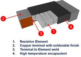
|
|
Q4. |
Regarding the power derating curve, what's the difference between terminal temperature and ambient temperature? |
|
A4. |
The derating curve used in Vishay Dale datasheets is based on ambient temperature. Shown on the chart, our parts will have their full power rating up to 70 °C. When the ambient temperature is above this temperature, the part will derate linearly to 0 W at 170 °C. 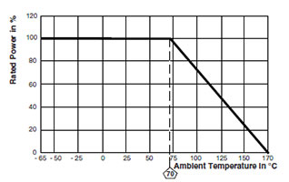
|
|
Q5. |
The maximum case temperature will reach 141 °C when 2.5 W maximum power is applied to the WSLF2512L5000FEA during the thermal test. Could you please help to determine whether this will result in any thermal risks? |
|||||||||||||||||||||||||||||||||||||||
|
A5. |
The thermal resistance is listed on the datasheet and is (hotspot - terminal temperature) / applied power. If the board lacks the sufficient thermal capacity to dissipate the energy generated in the resistance element, the device temperature will be excessive.
The full power rating of Power Metal Strip resistors is dependent upon the ability of the circuit board to dissipate the heat energy created in the resistance element. It is recommended to follow common design practices for power semiconductors that ensure the junction temperature is maintained within thermal limits by using large pad surfaces, thermal vias, heavier copper weights, and internal layers, as well as other thermal spreading features. The thermal resistance values provided function in the same manner as junction to terminal temperature. Below are the power vs temperature curves from which the thermal resistance was derived. 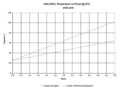
|
|||||||||||||||||||||||||||||||||||||||
|
Q6. |
How is the R value of shunt resistors measured? |
|
A6. |
This method is usually unreliable at these low resistance values because of probe placement error / variation. We measure the parts twice in the manufacturing process with "guard band" (a slightly tighter resistance limit than 1 %) to assure proper resistance value and tolerance. This is also done with precise probe placement (repeatable) and with specially designed resistance bridges. A possible consideration was suggested that measurement error could occur if you are measuring in a manner similar to the illustration below. In this case, we would expect to see the same amount of error, which is caused by the PCB design. 
Another possible cause is that during manufacturing we measure the parts unmounted and the solder process can change the "effective" probe / measurement location, which can cause the in-circuit measurement to differ slightly. And for resistance values below 0.01 Ω, measurement must be conducted with a precision resistance bridge that has the accuracy to measure these low value parts. Measurements are taken with a special 4-terminal test fixture and not manually placed test probes. The test fixture is required to ensure repeatable and accurate probe placement. Our test bridge is able to resolve to 0.000 000 10 Ω. |
|
Q1. |
What is a MELF resistor? What are the advantages of using a MELF resistor over a flat chip SMD resistor? |
|
A1. |
Metal electrode leadless face (MELF) resistors are cylindrical SMD devices. They offer superior SMD resistor performance in terms of accuracy, stability, reliability, and pulse load capability. The cylindrical construction of MELF devices provides an optimal power rating and pulse load capability related to the mounting space. Continuous development has led to improved long term stability and moisture resistance, and allows for high temperature operation to + 175 °C. MELF resistors with advanced pulse load capability are the perfect choice for the protection of circuitry with signal and mains input lines from surge pulses. They are also suitable for circuits exposed to high levels of electromagnetic interference or electro-static discharge. General SMD thick film resistors can be damaged and resistance value can be changed with high pulse loads. Typically, general SMD thick film resistors are used for pull-up and pull-down in digital circuitry. |
|
Q2. |
Can the worst-case resistance value change be calculated or estimated based on the estimated number of hours in operation? |
|
A2. |
The drift (ageing) of a resistor can be estimated using the Arrhenius equation. For example, on page 2 of the TNPW e3 datasheet, the customer can find the table "Maximum Resistance Change at Rated Dissipation." 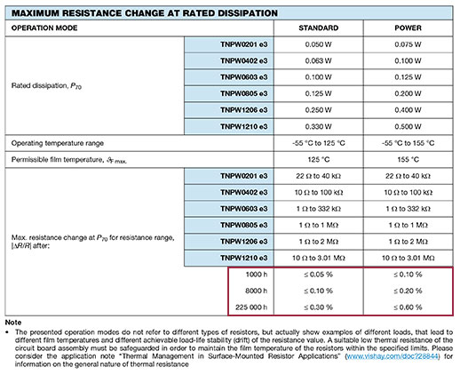
Here the maximum resistance changes for the different operation modes, as shown above. With the Arrhenius equation given below, the customer can estimate the resistance drift based on the specified resistance changes as stated in the datasheet: 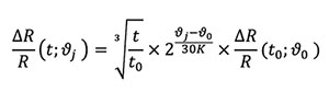
Example:
Parameters from the datasheet (standard operation mode) are: 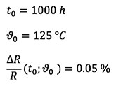
The requirements are 15 000 h at P70, so a full load at 70 °C ambient temperature: 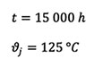
Drift estimation: 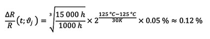
If the customer wants to use the resistance change as a worst-case parameter for an end of life tolerance, they could add up all the changes that can happen within their design. Even the resistance change is presumably lower. |
|
Q3. |
Apart from long time resistance drift, are there other parameters / conditions to be considered for the worst-case change in the resistance value? |
|
A3. |
Again, taking the example of the TNPW e3, page 9 of the datasheet gives specified permissible resistance changes depending on the different tests. The specified limits on these pages already represent the worst case; typical resistance changes are lower than these limits. So, the simple algebraic sum of permissible changes may represent the worst case, but this usually ignores statistical effects (in many cases these factors don't happen in the application at the same time or with full intensity). Therefore, it is reasonable to say that the root square sum method is considered to represent the most likely "worst case" deviation of the resistor over time. Considering influences like moisture (85 / 85), resistance to soldering heat, vibration, and ESD from page 9 and the following pages (which will affect the customer's application), the below estimation is the most probable worst-case stability: (4.25.1 Endurance, but as calculated above for 15 000 h: 0.12 % + 4.37 damp heat 85 / 85: 0.25 % + 4.18 resistance to soldering heat: 0.02 % + 4.22 vibration: 0.05 % + 4.38 ESD: 0.5 % = ΔR of 0.94 %) Root square sum method This was just an example, because it would be necessary to know what will affect the customer's application. Then you can use the specifications in the datasheet from the single tests. |
|
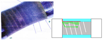
Q4. |
Why is the Vishay CRCW-HP more robust to pulse surges than competitors' double power mode thick film chip resistors? |
|
A4. |
As shown below, the internal resistance layers are on the top and bottom, so they are resistant to pulse surges. 
If you need more, please refer to the below link: |
|
Q5. |
When mounting a MELF resistor on the PCB, what kind of nozzle should be used in the pick and place machine? |
|
A5. |
If you replace the nozzle with a concave tip as shown below, you can vacuum and pick and place MELF resistors without a problem. 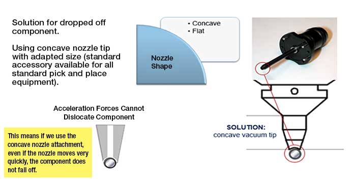
If you need more, please refer to the below link: |
|
Q6. |
How does a thin film chip resistor prevent a large aging drift of the resistance value in the final product (problem of electrolytic corrosion)? |
|
A6. |
Based on many years of manufacturing experience, Vishay DBR has fixed two types of countermeasures against failure modes in the end product.
If you need more information, please contact The Resistors University: |
|
Q7. |
There are two MELF operation modes: standard mode and power mode. What is the difference between them and how can I order the correct part? 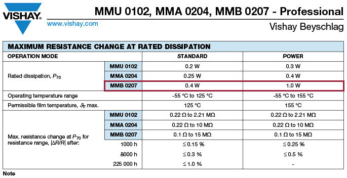
|
||||||||||||||||||||||||
|
A7. |
Please refer to the link below for details: In short, 2.1. Standard Operation Mode Under normal operating conditions in a typical circuit environment, a thin film SMD resistor would be operated with not more than 125 °C film temperature by not exceeding a suited maximum electrical load. The result would be a drift performance as outlined here: Thin film SMD resistor • standard operation
It is obvious that an SMD resistor operated under this condition is usable for over 20 years without causing trouble due to an excessive change of its value. 2.3. Power Operation Mode Not all applications of SMD resistors require the same life expectancy of over 20 years. Quite often, lifetimes of ten years are considered enough. This leads to a higher permissible drift and thus to the higher permissible film temperature of 155 °C. Thin film SMD resistor • power operation
Again, one single resistor product is suitable for two different classes of application by choice of the operating mode and the permitted power dissipation. |
||||||||||||||||||||||||
|
Q8. |
If we use the TNPV or MMA HV, how do we ensure that the creepage distance will be all right compared to using a few resistor pieces? |
|
A8. |
This has to be taken care of by the designer / engineer. One way to increase creepage distance is by having an air gap (slit) in the PCB material. If you need more information, please contact The Resistors University: |
|
Q1. |
What is the maximum rated power when a surface-mount thick film power resistor such as the D2TO35 / DTO25 is mounted on an ordinary PCB? |
||||||||||||||||||||||||||||||||||||||||||||||||||||||
|
A1. |
The theory of thermal resistance depends on the heat dissipation conditions of each customer's application (PCB material and number of layers, PAD size, etc.), but general indicators are as follows. Please see the application note for details.
|
|
Q2. |
What is the partial discharge of a power thick film resistor, and what are its effects? |
|
A2. |
Partial discharge is a localized electrical discharge that only partially bridges the insulation between conductors, and which can or cannot occur adjacent to a conductor. Partial discharges are a consequence of local electrical field (E) concentrations in the insulation or on the surface of the insulation. Partial discharges are essentially present in HV systems (generally > 1500 V). Corona is a form of partial discharge that occurs in gaseous media around conductors, which are remote from solid or liquid insulation.
|
|
Q3. |
What are the root causes of partial discharge failure? |
|
A3. |
|
|
Q4. |
What are the suggestions for customers when performing a partial discharge test? |
|
A4. |
|
|
Q5. |
The customer wants to know if the LTO150 can withstand 150 W for 0.3 s. According to the power curve in the datasheet, it seems that the LTO150 can withstand 450 W in 0.2 s. 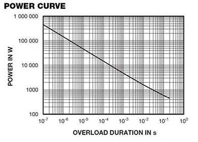
|
|
A5. |
After 0.2 s the heatsink starts to be important and the data given by R&D is based on an LTO150 mounted on a specific heatsink. The rules applied in the web tools are:
Thus, the LTO150 can actually withstand 90 J during 0.3 s, meaning 90 / 0.3 = 300 W, when mounted on a specific heatsink. |
|
Q1. |
What are the definitions of accuracy, resolution, and repeatability for non contacting position sensor? |
|
A1. |
Accuracy = linearity. It is equal to the maximum difference between the real function (of the sensor) and the theoretical function (= perfect function without error). For example, an accuracy of 13 bits corresponds to an error of 360 / 213 = 0.044°. 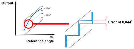
Resolution is the smallest moving step we can detect. For example, a resolution of 18 bits corresponds to the smallest step of 360 / 218 = 0.0014°. 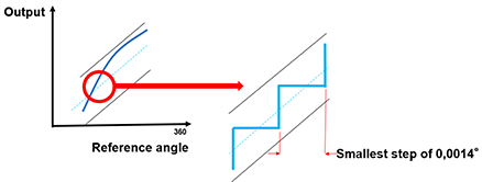
Repeatability is the difference between:
For example, a repeatability of 18 bits corresponds to 360 / 218 = 0.0014°. Vishay encoders have an excellent repeatability close to the resolution value! 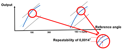
|
|
Q1. |
What is the principle of UIPMA and how does it work? |
|
A1. |
Principle 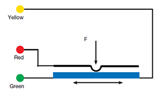
The voltage varies depending on the position of the object pressing on the deformable membrane. |
|
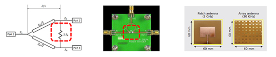
Q1. |
What is the main application for the CH? |
|
A1. |
In Wilkinson power dividers in massive MIMO antenna modules:
|
|
Q2. |
What is the suggested soldering process for the CH? |
|
A2. |
Soldering: The thickness, related to the surface of the pad, determines the quantity of solder that will form the joint during the reflow. The reflow has to be sufficient to obtain an ideal solder fillet at a 45° angle. The vapor phase reflow solder process uses flour carbon liquids, boiled to produce a vapor-saturated atmosphere, at a temperature slightly higher than the boiling point of the liquid and high enough to reflow the solder. The infrared reflow solder process uses heat energy produced by an infrared radiation source and by convection (natural or forced). In such a system, the heat time is dependent of the absorption coefficient of the material surface and of the thermal mass of all the components in relation to the surface available to the infrared radiation. The temperature of the components in an infrared oven is not precisely defined and temperature measurements should be taken on the component themselves when they are going through the oven. The temperature of small components may reach +260 °C when they are soldered at the same time as larger ones. The parameters that act on the temperature of the components are:
A standard profile of this process is given in the graph shown. A preheat period is necessary for the evaporation of all the volatile solvents contained in the solder paste before the action of the flux. It initializes the action of the flux on the solder and also on the metallic surfaces of the component terminations and substrate. 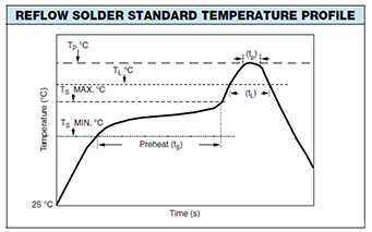
|
|
Q1. |
Why do Vishay's metal composite power inductors have lower EMI noise than the competition? |
|
A1. |
We use high permeability iron powder and press it hard, completely surrounding the coil and eliminating discrete gaps. This makes it possible for more lines of flux to be kept inside inductor body. The E-field shielded IHLE series can reduce EMI even further. Also refer to: |
|
Q2. |
Are there any precautions to take when mounting metal composite power inductors on the PCB? |
|
A2. |
Use the recommended lead (Pb)-free solder profile found online and follow the guidelines in the datasheet for PCB pad size. Bad solder joints may lead to vibration against the board and cause buzz noise. The IHLP itself is a solid composite part and does not cause vibration. Vias, or holes, under the inductor body are not recommend unless it is electrically insulated on the surface. It is best if it is covered with a solder- resistant material. If it is bare copper, moisture could be trapped between the inductor body and the vias, resulting in corrosion due to two dissimilar metals coming into contact with a liquid. There are no specific guidelines regarding how to design the inner layer traces when used on multi-layer PCBs. Also refer to: |
|
Q3. |
Is conformal coating on inductors permitted? Will it affect quality or reliability? |
|
A3. |
Conformal coating is a common practice and will not damage the IHLP series. It might affect the cooling of the IHLP, since the conformal coating may act as an insulator for heat dissipation. It is always good practice to test the temperature rise of all components under actual circuit operating conditions. |
|
Q4. |
What should the storage conditions for the IHLP series be? |
|
A4. |
Commonly, before mounting, high temperatures (or even low temperatures) can compromise the packaging (plastic carrier tape). Also, high temperatures can accelerate oxidation of the solder termination plating, affecting its solderability. However, IHLP series devices are vacuum-sealed, so only minimal oxidation will ever occur. There is no shelf life limit on our IHLPs with the original packaging and sealed packing bags. Once the part is mounted to the PCB, solderability and packaging is not a concern, so there is nothing to be compromised at the listed storage temperature. There are no specific conditions required during transportation. |
|
Q5. |
For the IHLP series, is it permissible to exceed the maximum voltage? |
|
A5. |
The maximum voltage rating for IHLP series inductors should not be exceeded, even under short term conditions. Once the limit is exceeded and actual breakdown occurs, the damage is done. However, the current rating for the inductors can be exceed under short pulse conditions. When a voltage breakdown occurs in an inductor, a low ohmic path is burned between its two terminals. Before the breakdown, the resistance between the terminals can be 1 MΩ or higher. So, there is effectively a 1 MΩ+ resistor in parallel with the inductor, and since it is 1 MΩ+, it has little if any effect on the performance of the inductor. When voltage breakdown occurs, the resistance becomes 100 kΩ or less, and now there is a resistive path between the terminals that can affect the inductor's performance. Also refer to: |
|
Q6. |
If there are differences in inductor lead lengths, would there be differences in the magnetic / electric field? |
|
A6. |
A large amount of shielding is done by the core. A short lead would have a smaller field; however, these parts are already very short, and the lead couldn't get much shorter. The lead will have a minimal effect on the field, similar to a trace on your board. Of course, you will need to test the part in your circuit to be sure that it will meet your field requirements. |
|
Q7. |
How should I define the differences between IHLP suffixes, like 01(A1), 11(1A), 51(5A), etc.? |
||||||||||||||||||||
|
A7. |
*A in the suffix stands for Automotive Grade part Also refer to: |
|
Q8. |
What is the difference between the rated current and saturation current of an inductor? |
|
A8. |
Rated current is the DC current that causes the inductor to increase by 40 °C from room temperature. This heating is caused by I^2R copper losses and does not take into account AC losses from the core and coil, which will also add to the temperature rise of the inductor. Saturation current (Isat) is the current where the inductance drops to some specified level. Vishay defines it as a 20 % shift downward from the inductance at zero DC current. The IHLP saturation is a soft, almost linear, drop in inductance. There is no sharp drop-off, as there is with ferrites. The slope of the saturation curve varies based on the powdered iron material (-A1, -1A, -5A, and -8A). For some materials and values, the Isat and the rated current is about the same (-1A and -5A). For a few values, the Isat might be less than the rated current. Some parts have rated current higher than the Isat. In these cases, you can operate them at currents above the 20 % saturation point without an excess temperature rise. It is best to consult the datasheet for details on the rated and saturation current for each P / N. Also refer to: |
|
Q9. |
Do IHLP inductors have problems with long term stability when working at high temperatures? |
|
A9. |
IHLP parts are not affected by temperature like ferrite inductors are. IHLP performance is virtually the same at different temperatures, as long as they are within the operating temperature range. If the temperature exceeds the maximum operating temperature, core losses could increase. The maximum continuous operating temperature for the -01 / -A1 and -11 / -1A materials is 125 °C. For the -51 / 5A and -81 / 8A materials, the maximum continuous operating temperatures are 155 °C and 180 °C, respectively. Also refer to: |
|
Q10. |
If we cannot find the suitable saturation current in the required size, what should we find next? |
|
A10. |
Vishay defines the saturation current (Isat) as a 20 % drop in inductance from the initial reading. Many competitors define the saturation current as a 30 % drop from the initial reading. If the 30 % saturation point is not listed on the Vishay datasheet, it can often be read from the graph on the datasheet or calculated with a simple linear extrapolation based on the 20 % saturation current. If we used a 30 % drop in inductance, the Isat would increase. Please reconsider the permissible inductance drop. |
|
Q1. |
How can we get the Vishay NTC thermistor R-T table? |
|
A1. |
Please let the Vishay Product Marketing team (or NLR@vishay.com) know your specific SAP PN or model, temperature range, and temperature interval step. Alternatively, you can download the R-T Calculator Excel file yourself. "My Vishay NTC Curve" provides a resistance temperature table for every NTC thermistor available from Vishay. This tool can be downloaded to any computer that runs MS Office Excel. |
|
Q2. |
At what temperature does the NTCS detect an extreme ambient temperature difference between the top and bottom side? 
|
|
A2. |
The situation described in the image is a complex temperature or heat-flow pattern, which depends upon the heat transfer on both sides (top and bottom) of the SMD NTC. In order to make a prediction, we would need to quantify the whole thermodynamic environment, including the PCB, solder-lands and tracks, solder paste, air conditions on the top side, etc. On the simple image shown above (without a PCB
mount), the situation can be simplified: In reality the component (NTCS, NTCAFLEX, or NTCALUG) will be fixed to a surface and the average temperature that will be seen by the NTC thermistor chip will depend on the heat flow in and out of the component. In the example of a NTCAFLEX in the image below, the given temperature levels are just provided as an indication. In reality everything will depend on the different thermal resistances between the different layers and materials: hot plate → flex foil → NTC chip → glob top → air 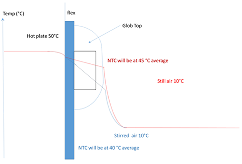
|
|
Q3. |
Questions about R-T tables. 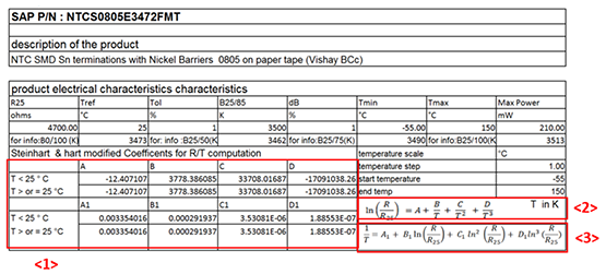 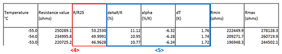
|
|
A3. |
Question 1 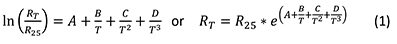
to calculate RT as a function of temperature (T in Kelvin) by replacing A, B, C, and D with their table values (for example, -12.407..., 3778... etc.) and replacing the R25 value by the exact or nominal value at 25 °C. You can compute R at any temperature in the specified operating range and will obtain the exact values of the table R as a function of T (T= temperature in K or in °C +273.15). The A1, B1, C1, and D1 coefficients are used in the formula to calculate temperature out of resistance (RT): 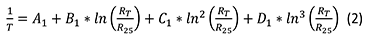
For most NTC types or curves there is only one set of coefficients (A, B, C, and D and A1, B1 , C1, D1) independent of the temperature range (< 25 °C or > 25 °C). However, for a few NTC types with more complex curves, we have two sets of coefficients: one set for temperatures < 25 °C and another for temperatures > 25 °C. In the example table for the NTCS0805 4K7, there is only one set. Question 2 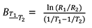
Question 3 B values are defined by their different ceramic compositions. It is good practice to calculate B-values at other temperatures, like B0/100 or B25/50, which are used by other suppliers. In the example table, we mention four alternative B values — B0/100 = 3473 K, B25/50 =3462 K, B25/75 = 3490 K or B25/100 = 3513 K — for the original B25/85 = 3500 K. Question 4 Question 5 The temperature coefficient (TCR) is called the Alfa (α) for NTC thermistors and it is expressed in % / °C or % / K (1 °C = 1 K) and it is dependent on the temperature. The RT tolerance or Delta R / R divided by the Alfa (α) will give you the Delta T (dT), the accuracy with which that temperature can be measured, or dR / R = Alfa*dT. So in the table at -55 °C, this NTCS0805 4K7 1 % can measure -55 °C with an accuracy of ± 11.12 / 6.32 = ± 1.76 °C (or K). So, if we look at it in function of temperature, the components will have a value of 250289.1 Ω at a temperature of -55 °C ± 1.76 °C. |
|
Q4. |
Are NTC products sensitive to electrical overstress (EOS) such as ESD, and what capabilities can we suggest? |
|
A4. |
NTC products are not sensitive to ESD, since their internal structure is not "multi-layer." The ESD level these components can resist is > 25 kV air discharge (HBM). NTCs are sensitive to overpowering in constant voltage mode: always measure NTCs with controlled current and power, never control an NTC with a fixed voltage, as this will possibly result in thermal runaway. |
|
Q5. |
How should a NTC resistance value be selected for an application? |
|
A5. |
The general rule is to use a low resistance sensor for a low temperature application and a high resistance sensor for a high temperature application. The goal is to have a suitable working resistance value in the temperature range of interest. For many applications a 10 kΩ thermistor is a good compromise for low and higher temperature measurements or controls. |
|
Q6. |
How fast do NTCs respond? |
|
A6. |
Response time is defined as the time it takes to reach 63.2 % of the temperature difference when the thermistor is exposed to a sudden temperature jump: for example, from 25 °C in air to 85 °C in water or oil. The response time is dependent on the thermal mass of the component and also the design of the part. The smaller the sensor, the faster the response time. A discrete sensor will respond faster than the same sensor packaged inside a metal or plastic housing. |
|
Q7. |
There are two temperature ranges specified: one at zero power and another at maximum power. What are these for?
|
|
A7. |
We define two temperature ranges (0 to 55 °C: 100 % rated power allowed), then outside this temperature range linear derating has to be applied until 1 % of the maximum specified power is reached (which is the zero-power condition). 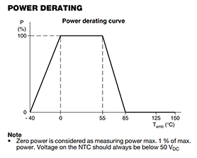
|
|
Q8. |
For the NTCS0805 thermistor, the power rating given in the datasheet is 210 mW, while the power rating given for the leaded type is 100 mW. Why is there such a difference? |
|
A8. |
In some leaded thermistors (NTCLE300, -301, -213, and -305), we deal with much thinner wires and with low thermal conductivity, so those types also have a lower dissipation factor (D-factor like 0.8 mW/K for the NTCLE305). The chips of the NTCLE305, for example, are also smaller than the chips used in the NTCLE300. So to limit the maximum temperature those NTC thermistors can reach when electrical power is applied to them, we limit the maximum power to 100 mW, for example, or sometimes 50 mW, like for the NTCLE305. However, the NTCLE100 leaded series with thick copper wire is are defined with 500 mW maximum power, as the devices' dissipation factor is also much higher at 7 mW/K or 8.5 mW/K. The maximum power (100 % P) is generally the power that drives the part up to the maximum temperature at the specified ambient temperature. The NTCS0805 has a rather high D-factor when solder-mounted on an epoxy PCB, so the power can be higher: 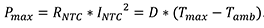
Pmax for the NTCS0805 = 210 mW at 25 °C. This power will let the NTCS average body temperature increase with 210 mW / 3.5 mW/K = +60 °C and will reach 85 °C on average. |
|
Q9. |
How are NTC thermistors measured? |
|
A9. |
The published R-T values are measured at the temperature T. The published B25/85 value is the result of the R measurement at 25 °C and at 85 °C. Hence, these temperatures and values should be used when checking. The following general precautions have to be taken when measuring NTC thermistors with high precision:
|
|
Q10. |
For the NTCC wire bonding type, will silver plating impact weldability? |
|
A10. |
The electrode (thickness ≈ 13 µm) is specially designed for wire bonding. Some dopes are added to optimize the bond ability. Use a solder paste material with around 3 % silver, in order to prevent the metallization dissolution into the solder material, or apply silver sintering. |
|
Q1. |
What is the TCR for various resistor element materials? |
||||||||||||||||||||||||||||||||||||||||
|
A1. |
The TCR table for various resistor element materials is below.
|
||||||||||||||||||||||||||||||||||||||||
|
Q2. |
What is the recommended soldering profile for axial leaded resistors, such as the CW02 series? |
|
A2. |
The soldering profile is provided below. 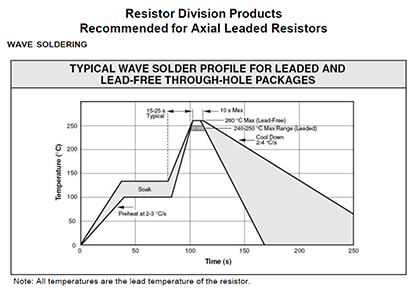
|
|
Q3. |
What information should be considered when reviewing pulse handing resistors? |
|
A3. |
|
|
Q4. |
What is the meaning of 0.05 Ω in the test limit of ± (5.0 % + 0.05 Ω) ΔR?
|
|||||||||||||
|
A4. |
The 0.05 Ω is an ohmic adder that's given to account for different bridges and the difference between how people use the bridges to read the resistance value. This would be a worst-case change from one bridge to another when measuring the resistance value. The ohmic adder is also from earlier datasheet generations, where instrument resolution was not as low as it is today. The ohmic adder was an allowance for military specifications. |
|||||||||||||
|
Q5. |
What is the power derating curve of a resistor and what does it mean? |
|
A5. |
The rated dissipation at P70 is the maximum permitted power load at an ambient temperature of 70 °C. Applying rated power of P70 on the resistor leads to a temperature increase that results in a film temperature, which corresponds to the specified permissible film temperature. An increased film temperature leads to aging of the resistor, resulting in resistance drift. The specified rated dissipation and permissible film temperature ensure that resistance stability limits are not exceeded. The definition of the rated dissipation at 70 °C has historic reasons and is specified in the generic specification IEC60115-1 for fixed resistors. The derating curve shows the maximum allowable dissipation at ambient temperatures within the operating temperature range. It is verified by thermographic measurement of the resistive film hot spot temperature. If ϑ_amb > 70 °C, the power load has to be derated to avoid exceeding the maximum permissible film hot spot temperature. Because it would be necessary to know what will affect the customer's application, you can use the specification in the datasheet of the single tests. Temperature ranges: 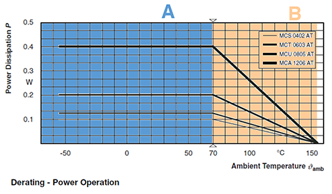
A area: according to IEC 60115-1, the rated dissipation between the minimum operating temperature and 70 °C is shown above. B area: power dissipation is derated so that the resulting temperature increase ([Δϑ = R](th JA)∗P) plus the ambient temperature do not exceed the permissible film temperature. If you need more information, please contact The Vishay Resistor University: |
|
Q6. |
What is the voltage coefficient of a high voltage resistor? |
|
A6. |
Because of the applied voltage to the resistor, especially the high voltage, the resistance value will change. The change in the resistance value is determined by the "voltage coefficient" of the resistor, often called VCR. VCR is expressed in ppm / V. Below is the typical test procedure for measuring VCR. The maximum allowed voltage, U1, is applied to the resistor and the resistance (R1) is measured. After that 1/10 of U1 is applied (U2) and the resistance (R2) is measured. (The temperature of the resistor should be kept constant while determining the VCR of a resistor. This is to avoid TCR influence on the resistance value). The VCR is calculated as: 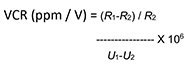
If you need more information, please contact The Vishay Resistor University: |
|
Q7. |
What is the difference between discharge and active discharge in EV inverters? |
||||||||||||||||||||||||
|
A7. |
Discharge: the resistor is used to discharge capacitors during switch off or fault (all the energy is dissipated in one shot). There is a large range of ohmic values (from a few Ω to a few kΩ), typical duration of 100 ms to 1 s, and there is no average power. A large resistor is needed for energy handling. Active discharge: the capacitor discharges during switch-off or fault. A global discharge energy is the same as for a classic discharge, but is dissipated step by step (= multiple pulses). Active discharge allows for the application of a continuous power dissipation on the resistor, avoiding entering overload conditions as much as possible. A transistor and PWM command switch the current with high frequency (∼1 kHz) pulses. In the case of a connected battery, the dissipated power is limited, and the temperature remains low. Classic discharge vs. active discharge with
PWM 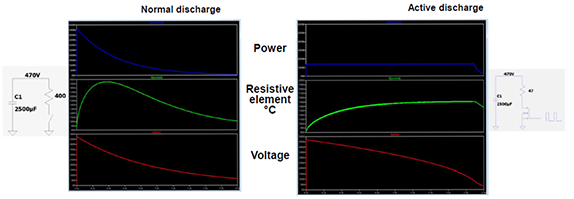
Why are thick film resistors recommended for active discharge?
|